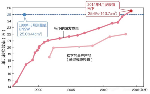
The cell conversion efficiency of the crystalline silicon solar cell was refreshed at the highest level in 15 years. Crystalline silicon is currently the mainstream way of solar cells. The previous highest value was 25.0% that was created by the University of New South Wales (UNSW) in 1999, and Matsushita hit a new record of 25.6% (Figure 1).
Panasonic not only updated the highest value. UNSW's record was achieved in a compact unit with an area of ​​only 4cm2, while Panasonic was implemented on a practical size solar cell of 143.7cm2. Panasonic also prototyped a module using 72 such cells. As a result, the module output power is about 270W, which is 25W higher than the company's latest product.

Figure 1: Conversion efficiency exceeds 25%
Using new structures to initiate challenges
The theoretical efficiency of crystalline silicon solar cells is about 29%, and 25 to 26% basically reach the limit Note 1). As Panasonic achieves the conversion efficiency of the limit range, the degree to which the conversion efficiency of the crystalline silicon solar cell can be improved has attracted the attention of the solar cell industry. Panasonic also plans to further increase conversion efficiency, the company's head said, "The next goal is to achieve 26%. This value should be achieved."
Note 1) Among incident light energy sources, 20 to 30% are transmission losses, about 30% are quantum losses, and about 10% are carrier recombination, surface reflection loss, and series resistance loss.
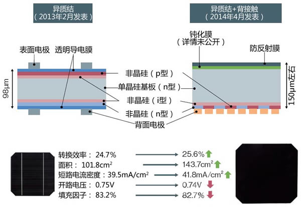
With the improvement of conversion efficiency at the same time by the attention of the solar cell industry, is to achieve the conversion efficiency of the cell structure of 25.6%. Panasonic has previously used a "heterojunction" structure that forms an amorphous silicon layer on a silicon wafer. The effect of inhibiting carrier recombination through the effect of the amorphous silicon layer helps to increase the voltage. Electrodes are disposed on the light receiving surface and the back surface, respectively.
For the first time, Panasonic adopted a “back contact structure†that retained part of the heterojunction and removed the light-receiving surface electrode. Since the light blocking electrode is removed, the amount of current can be increased. In fact, the short-circuit current density as a current value target is improved compared with the company's heterojunction unit released in February 2013 (Fig. 2). Note 2). While maintaining the high voltage using the heterojunction, the method of increasing the current through the back contact structure contributes to achieving a conversion efficiency of 25.6%.

Figure 2: Implementation with a different structure than before
Note 2) But the open circuit voltage drops. Panasonic is analyzing the reasons. It may be affected by the increase in wafer thickness.
It's not just Panasonic that is working on both the fusion heterojunction and the back contact. Sharp and South Korea’s LG Electronics are also promoting research and development. Among them, Sharp used a small-area unit to achieve 21.7% unit conversion efficiency in 2012, and quickly increased to 24.7% in 2013. In April 2014, the company announced a 25.1% efficiency note3). Since more than 25% of the results have been issued successively, it is estimated that the research and development of this structure will become more and more active.
Note 3) The area is 3.72 cm2, the short-circuit current density is 41.7 mA/cm2, the open circuit voltage is 0.736 V, and the fill factor is 81.9%. In addition, Sharp has actually applied a back contact structure in its products.
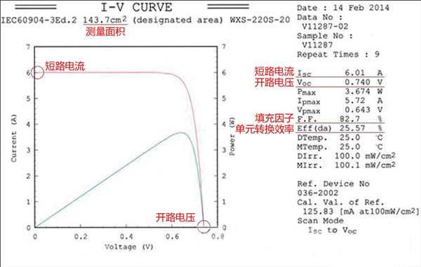
However, Panasonic has not yet decided whether to apply this new structure in its products. However, "the method of improving efficiency has added a kind" (Panasonic). The company began to advance research a few years ago and this time finally achieved a conversion efficiency of more than 25% (Figure 3). Although the potential for improvement of conversion efficiency is high, when it is actually put into operation, it is necessary to add a backside pattern process or the like to the cell production line, or to improve the modular process. Note 4).

Figure 3: Measurements in February 2014
Note 4) The structure of the heterojunction is symmetrical on the front and back sides, and the stress is small, which is conducive to thinning. The use of a back contact structure loses this advantage, but Matsushita stated that "stress can be controlled by taking care of the unit structure." The company has not yet begun to promote thinning. This time, we use wafers that are basically the same as the mass production products, and therefore have a thickness of about 150 μm.
Panasonic is currently continuing to promote the research and development of heterojunction units. The company stated that "the conversion efficiency has a potential of more than 25%." At present, heterojunction cells are more focused on using them to manufacture volume products than to increase conversion efficiency.
Air Conditioner Bracket,Aircon Bracket,Ac Support Bracket,Air Conditioner Support Bracket
LONG TERM ELEC. CO., LTD , https://www.longterm-hvac.com