With the support of the Swiss National Science Foundation, researchers invented a new technique for engraving materials to build micromechanical systems. The most special part of them is that they use artificial monocrystalline diamond to produce an extremely small watch component.

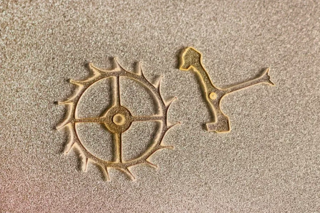
Diamond is hard, tough, has good thermal conductivity, and is highly transparent, making it an ideal material for many mechanical equipment and optical devices. At the same time, however, it is very challenging to accurately cut diamonds in micrometers (thousandths of a millimeters). Under the auspices of the Swiss National Science Foundation, Professor Neils Quack from the Federal Institute of Technology in Lausanne, Switzerland, and his team invented a new method for engraving a micromechanical watch system from artificial single crystal diamonds. The escape wheel and the pallet fork are three millimeters in diameter.

Escape wheel, made of synthetic diamond, 3mm wide.
The "Reactive Ion Etching" technology is widely used in the field of computer chips. The team has improved this technology by successfully etching the synthetic diamond into a three-dimensional shape of 0.15 mm thick, which is three times thicker than the thickest structure. “We are gradually approaching the standard thickness of the watch industry, which is 0.2 mm,†Quack said. “This technology has caught the attention of the industry. We are currently negotiating with a Swiss watch company. We believe that diamond can reduce friction and increase power reserve. That is, extending the time that the watch needs to be wound again. However, this is only a hypothesis to be confirmed." In the watch industry, diamond has Other advantages: it has transparency, it can be colored, and in addition, the diamond is non-magnetic. It is also a highly sought after property in the current market.

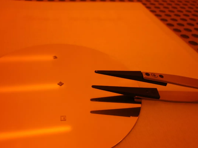
The tip of the tweezers is a diamond escape wheel with a diameter of 0.75 mm and a silicon wafer underneath, which serves as a support during assembly.

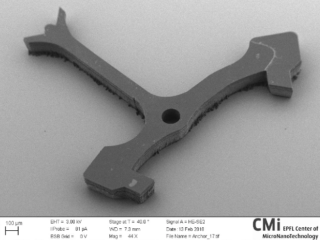
A single-piece synthetic diamond watch component pallet.
Industrial patent
Previously, because the ions (charged atoms) accelerated in the electric field, not only the diamond layer at the selected position was moved, but also the film with the specified target shape was eroded. The "reactive ion etching" technique can only produce a structure with a thickness of 0.05 mm. . Therefore, the thickness of the resulting structure is limited by the resistance and thickness of the film. In less than half a year, a research assistant named Adrien Toros of the Institute of Microelectronics at the Federal Institute of Technology in Lausanne, Switzerland, invented a two-layer film consisting of a layer of aluminum and a layer of silicon dioxide. The layer can adsorb diamond well, and the outer silica layer is thicker and more resistant to the influence of ion reaction. This technology speeds up the etching process and achieves near-vertical deep cuts.
With the support of Innosuisse (previously CTI), the team plans to work with Swiss diamond manufacturer Lake Diamond, who have previously applied for a patent. Pascal Gallo, the company's CEO, said: "In the medium term, we will use this technology to accurately produce and commercialize micron-sized components to expand our manufacturing sector."
In addition, another project is underway, and researchers are working on making optical components from ultrapure diamonds, such as lenses that can be operated in the infrared spectrum during thermal imaging, and laser devices used in industrial cutting.
Niels Quack said: “When I started this research in 2015, I never imagined these industrial applications. But thanks to the support of the Gebert Rüf Stiftung Foundation, we quickly saw the prospects of the project and then successfully developed it. A practical industrial application. For me, this perfectly proves that basic research often brings some unexpected applications, which is very attractive for the industrial field. Keeping thinking open is too important!"
The study was conducted at the Federal Institute of Technology in Lausanne, Switzerland, and was supported by the Swiss National Science Foundation's SNSF Professorship (this fund program has now been changed to SNSF Eccellenza Professorial Fellowhips). The project was also supported by the Gebert Rüf Stiftung Foundation and Lake Diamond in Yverdon, which provided artificial single crystal diamond. Pascal Gallo, the company's CEO, is the co-author of the paper. These components were assembled at the Micro-Nano Technology Center at the Federal Institute of Technology in Lausanne, Switzerland.
Other
Dongguan Huitong Automatic Machinery Technology Co., Ltd , https://www.breezesolution.com